SmoothBacklight: a Hardware Mod for Improving Backlight PWM Frequency of Your TV
Ever noticed eye strain or headache after watching your Samsung LED TV? A likely reason for this is an invisible picture flickering. Samsung F-series LED TVs (maybe all previous series too) use pulse width modulation (PWM) to adjust brightness of white backlight LEDs. On TV model UE55F6500 the backlight turns on an off 100 times per second. For F7xxx and F8xxx models the PWM frequency is a bit higher, subjectively around 200Hz. These frequencies are way too low for a comfortable watching. More about PWM-related health issues here.
This page describes an inexpensive do-it-yourself hardware modification that increases backlight PWM frequency to a more comfortable level of 2.2kHz. This method is only suitable for TV models without the Micro Dimming feature.
WARNING: THIS MOD CAN DAMAGE YOUR TV AND EVEN LEAD TO A FIRE IN YOUR HOUSE! USE AT YOUR OWN RISK. AUTHORS AND WEBPAGE ADMINISTRATORS BEAR ABSOLUTELY NO RESPONSIBILITY.
- What you get
- the picture is perceived smoother and with less discomfort. In long term, you get a healthier family. Backlight adjustment works as normal. Future MSP430 code update is possible without TV disassembly.
- What you loose
- 3D is unusable due to a severe crosstalk. All dynamic dimming features must be disabled from the menu because the dimming adjustment lags. You might loose warranty depending on how inaccurate you are. At last, a more frequent switching "wears down" backlight LEDs and driver circuitry faster. Power transistors in LED driver warm up to 45C, which is about 13C warmer than before (however some transistors in power supply warm to 67C both before and after the mod). Hence the warning above. Good air flow behind the TV is essential for cooling.
Modification Procedure
Required hardware: one TI MSP-EXP430G2 Launchpad development kit ($10 from TI), one 56k or 470k resistor, some wiring, a Phillips screwdriver, a small-pitch flat-blade screwdriver, a multimeter and a soldering iron.
The modification is explained for TV model UE55F6500. I have no experience with other models, but should be the same principle as long as there's no micro dimming feature.
- The VCC internal voltage generated on MSP-EXP430G2 Launchpad is 3.6V. To lower it to 3.3V replace R8 by 56k (or solder 470k in parallel with the installed R8 resistor). Since the pads for R8 are so small, I poured some epoxy on the re-soldered resistor to avoid accidental tear off. Finally, make sure the VCC voltage does not exceed 3.3V.
- Flash executable code to MSP430. Download compiled code here: smoothbacklight.out.
- On Linux: connect the Launchpad to a USB port, then run:
- sudo apt-get install mspdebug
- sudo mspdebug rf2500 "prog smoothbacklight.out" exit
- Or on Windows: use TI Code Composer Studio to (modify, recompile and) flash the code.
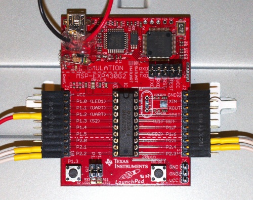
- Solder wires to the Launchpad pins as shown below.
- TP3: GND
- TP1: +5V
- P1.2: PWM_IN
- P2.1, P2.2, P2.4 and P2.5: PWM_OUT
- Optional: if you have an oscilloscope, test how the thing works: input a 3.3V PWM signal to pin P1.2 (e.g. from the scope's test terminals) and observe output on pins P2.1, P2.2, P2.4 and P2.5.
- Disconnect power from TV.
- Unscrew and remove the back cover. You see two printed circuit boards:
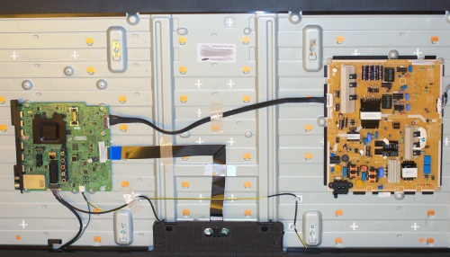
- A mainboard (on the left) is connected to a power supply / backlight LED driver board (on the right).
- Front side of the LED driver board:
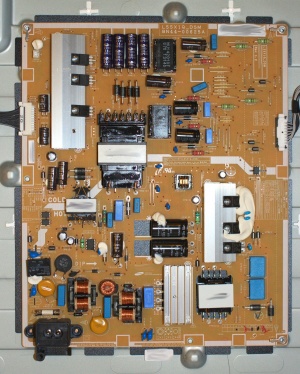
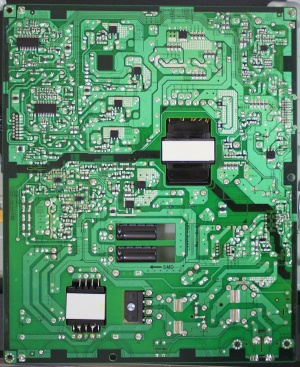
- Back side of the LED driver board:
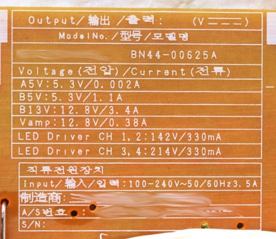
- PSU and LED driver specs are printed on the board:
- The LED driver has four channels. They are controlled by P_DIM1, ..., P_DIM4 lines of the 20-wire cable. Connector pinout:
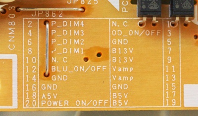
- The signal on P_DIM lines: 0V = LED is off, 3.3V = LED is on. The mainboard sends a 100Hz PWM signal on all lines. Prior to firmware version 1112 the maximum backlight setting produced a 40% PWM duty cycle. Current firmware uses full brightness, i.e. 100% duty cycle.
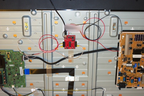
- Mount the Launchpad on the TV using a double-sided tape:
- Connect GND (TP3) to TV chassis and +5V (TP1) to B5V.
- The Launchpad, being a PWM signal converter, should be connected between the mainboard and the LED driver board. So, detach the four P_DIM pins 2, 4, 6 and 8 from one side of the 20-wire cable. Use a small-pitch flat-blade screwdriver to accurately remove the pins from the connector housing. Connect any of the four P_DIM signals coming from the mainboard to PWM_IN (P1.2) on the Launchpad. Connect the four PWM_OUT signals (P2.1, P2.2, P2.4 and P2.5) to the P_DIM pins on the LED driver board.
- Test the TV, make sure the backlight adjustment works.
- Attach a USB cable to Launchpad.
- Lead the USB cable through any available opening in the TV back cover and install the back cover. The USB cable is useful for future MSP430 code updates: flash while the TV is turned off.
Source Code
/* LED LCD backlight PWM frequency converter. Developed for Samsung UE55F6500 TV.
 * Code for TI MSP430G2553 20-pin package installed into the LaunchPad board MSP-EXP430G2.
 *
 * Takes any PWM signal on input.
 * Output frequency is OUTFREQ.
 * Output duty cycle is scaled by factor OUTMAXDUTYCYCLE/INMAXDUTYCYCLE. Max is OUTMAXDUTYCYCLE.
 * LED1 is toggled when input signal is constant (0% or 100% duty cycle).
 * LED2 is toggled when duty cycle is measured and set.
 *
 * Pin usage:
 * Input PWM signal: pin 4 (P1.2).
 * Output PWM signal: pins 9 (P2.1), 10 (P2.2), 12 (P2.4) and 13 (P2.5).
 * LaunchPad LEDs: pin 2 (P1.0) and pin 14 (P1.6).
 *
 * Required VCC voltage: 3.3V.
 * The voltage on MSP-EXP430G2 is 3.6V. To adjust it replace R8 by 56k and measure voltage.
 */

#include <msp430.h>

#define INSAMPLES        31      // number of samples to average input duty cycle measurement over, max 650
#define INMAXDUTYCYCLE   100     // input duty cycle that is mapped to OUTMAXDUTYCYCLE, per cent. Lower results are scaled accordingly
#define OUTMAXDUTYCYCLE  100     // max output duty cycle, per cent
#define OUTFREQ          2237    // output frequency, Hz, max 80000
#define MAXOVERFLOWS     2       // number of consecutive timer overflows to detect constant signal

unsigned int samples, accumulatedDutyCycle, rEdge, fEdge, overflows;
const unsigned int period = 8000000/OUTFREQ;

inline void set_duty_cycle(unsigned char p)         // takes value in per cent
{
	if ( p > OUTMAXDUTYCYCLE ) p = OUTMAXDUTYCYCLE;
	unsigned int duty = ((unsigned long)period*p)/100;

	/* TA1CCR1, Timer_A Capture/Compare Register 1 */
	TA1CCR1 = duty;

	/* TA1CCR2, Timer_A Capture/Compare Register 2 */
	TA1CCR2 = duty;
}

/*
 * main.c
 */
int main(void) {

    WDTCTL = WDTPW | WDTHOLD;	// Stop watchdog timer

    /* Port 1 Output Register */
    P1OUT = 0;

    /* Port 1 Port Select Register */
    P1SEL = BIT2;

    /* Port 1 Direction Register */
    P1DIR = BIT0 | BIT6;

    /* Port 1 Resistor Enable Register */
    P1REN = 0;

    /* Port 1 Interrupt Edge Select Register */
    P1IES = 0;

    /* Port 1 Interrupt Flag Register */
    P1IFG = 0;

    /* Port 2 Output Register */
    P2OUT = 0;

    /* Port 2 Port Select Register */
    P2SEL = BIT1 | BIT2 | BIT4 | BIT5 | BIT6 | BIT7;

    /* Port 2 Direction Register */
    P2DIR = BIT1 | BIT2 | BIT4 | BIT5;

    /* Port 2 Interrupt Edge Select Register */
    P2IES = 0;

    /* Port 2 Interrupt Flag Register */
    P2IFG = 0;

    /* Port 3 Output Register */
    P3OUT = 0;

    /* Port 3 Direction Register */
    P3DIR = 0;

    /*
     * Basic Clock System Control 2
     *
     * SELM_0 -- DCOCLK
     * DIVM_0 -- Divide by 1
     * ~SELS -- DCOCLK
     * DIVS_0 -- Divide by 1
     * ~DCOR -- DCO uses internal resistor
     *
     * Note: ~<BIT> indicates that <BIT> has value zero
     */
    BCSCTL2 = SELM_0 | DIVM_0 | DIVS_0;

    if (CALBC1_8MHZ != 0xFF) {
        /* Adjust this accordingly to your VCC rise time */
        __delay_cycles(100000);

        // Follow recommended flow. First, clear all DCOx and MODx bits. Then
        // apply new RSELx values. Finally, apply new DCOx and MODx bit values.
        DCOCTL = 0x00;
        BCSCTL1 = CALBC1_8MHZ;      /* Set DCO to 8MHz */
        DCOCTL = CALDCO_8MHZ;
    }

    /*
     * Basic Clock System Control 1
     *
     * XT2OFF -- Disable XT2CLK
     * ~XTS -- Low Frequency
     * DIVA_0 -- Divide by 1
     *
     * Note: ~XTS indicates that XTS has value zero
     */
    BCSCTL1 |= XT2OFF | DIVA_0;

    /*
     * Basic Clock System Control 3
     *
     * XT2S_0 -- 0.4 - 1 MHz
     * LFXT1S_0 -- If XTS = 0, XT1 = 32768kHz Crystal ; If XTS = 1, XT1 = 0.4 - 1-MHz crystal or resonator
     * XCAP_1 -- ~6 pF
     */
    BCSCTL3 = XT2S_0 | LFXT1S_0 | XCAP_1;

    /*
     * TA0CCTL0, Capture/Compare Control Register 0
     *
     * CM_3 -- Both Edges
     * CCIS_0 -- CCIxA
     * ~SCS -- Asynchronous Capture
     * ~SCCI -- Latched capture signal (read)
     * ~CAP -- Compare mode
     * OUTMOD_0 -- PWM output mode: 0 - OUT bit value
     *
     * Note: ~<BIT> indicates that <BIT> has value zero
     */
    TA0CCTL0 = CM_3 | CCIS_0 | OUTMOD_0;

    /*
     * TA0CCTL1, Capture/Compare Control Register 1
     *
     * CM_3 -- Both Edges
     * CCIS_0 -- CCIxA
     * SCS -- Sychronous Capture
     * ~SCCI -- Latched capture signal (read)
     * CAP -- Capture mode
     * OUTMOD_0 -- PWM output mode: 0 - OUT bit value
     *
     * Note: ~SCCI indicates that SCCI has value zero
     */
    TA0CCTL1 = CM_3 | CCIS_0 | SCS | CAP | OUTMOD_0 | CCIE;

    /*
     * TA0CTL, Timer_A3 Control Register
     *
     * TASSEL_2 -- SMCLK
     * ID_3 -- Divider - /8
     * MC_2 -- Continuous Mode
     */
    TA0CTL = TASSEL_2 | ID_3 | MC_2 | TAIE;

    /*
     * TA1CCTL1, Capture/Compare Control Register 1
     *
     * CM_0 -- No Capture
     * CCIS_0 -- CCIxA
     * ~SCS -- Asynchronous Capture
     * ~SCCI -- Latched capture signal (read)
     * ~CAP -- Compare mode
     * OUTMOD_7 -- PWM output mode: 7 - PWM reset/set
     *
     * Note: ~<BIT> indicates that <BIT> has value zero
     */
    TA1CCTL1 = CM_0 | CCIS_0 | OUTMOD_7;

    /*
     * TA1CCTL2, Capture/Compare Control Register 2
     *
     * CM_0 -- No Capture
     * CCIS_0 -- CCIxA
     * ~SCS -- Asynchronous Capture
     * ~SCCI -- Latched capture signal (read)
     * ~CAP -- Compare mode
     * OUTMOD_7 -- PWM output mode: 7 - PWM reset/set
     *
     * Note: ~<BIT> indicates that <BIT> has value zero
     */
    TA1CCTL2 = CM_0 | CCIS_0 | OUTMOD_7;

    /* TA1CCR0, Timer_A Capture/Compare Register 0 */
    TA1CCR0 = period - 1;

    set_duty_cycle(0);

    /*
     * TA1CTL, Timer_A3 Control Register
     *
     * TASSEL_2 -- SMCLK
     * ID_0 -- Divider - /1
     * MC_1 -- Up Mode
     */
    TA1CTL = TASSEL_2 | ID_0 | MC_1;

    // Variable Initialization
	rEdge = 0x00;
	fEdge = 0x00;
	samples = 0x00;
	accumulatedDutyCycle = 0x00;
	overflows = 0x00;

	while(1)
	{
	    /*
	     * SR, Status Register
	     *
	     * ~SCG1 -- Disable System clock generator 1
	     * ~SCG0 -- Disable System clock generator 0
	     * ~OSCOFF -- Oscillator On
	     * ~CPUOFF -- CPU On
	     * GIE -- General interrupt enable
	     *
	     * Note: ~<BIT> indicates that <BIT> has value zero
	     */
		__bis_SR_register(LPM1_bits + GIE);       // Enter LPM1
	}
	return 0;
}

// TA0_A1 Interrupt vector
#pragma vector = TIMER0_A1_VECTOR
__interrupt void TIMER0_A1_ISR (void)
{
	switch(__even_in_range(TA0IV,0x0A))
	{
		case  TA0IV_NONE: break;              // Vector  0:  No interrupt
		case TA0IV_TAIFG:					  // Vector 10:  TAIFG timer overflow
			if ( rEdge == 0x00 )              // No edges have been detected in last period
			{
				overflows++;
				P1OUT ^= BIT0;                // Toggle LED1
			}
			rEdge = 0x00;
			fEdge = 0x00;
			if (overflows>=MAXOVERFLOWS)      // Input is either permanently high or low
			{
				/*
				 * There's no external pulldown resistor on P1.2.
				 * Internal pulldown doesn't work when pin is not GPIO.
				 * When disconnected, the pin is at 2.5V and reading is unreliable.
				 */
				if(P1IN&BIT2) set_duty_cycle(OUTMAXDUTYCYCLE);
				else set_duty_cycle(0);
				accumulatedDutyCycle = 0x00;
				samples = 0x00;
				overflows = 0x00;
			}
			break;
		case  TA0IV_TACCR1:                   // Vector  2:  TACCR1 CCIFG
			if ( TA0CCTL1&COV )               // Capture overflow
			{
				rEdge = 0x00;
				fEdge = 0x00;
				TA0CCTL1^=COV;				  // Reset the overflow flag
			}
			else
			{
				if (TA0CCTL1 & CCI)             // Rising edge was captured
				{
					if ( (rEdge!=0x00) && (fEdge!=0x00) && (fEdge>rEdge) )
					{
						accumulatedDutyCycle += (unsigned long)(fEdge-rEdge)*100/(TA0CCR1-rEdge);
						samples++;
						if (samples >= INSAMPLES)
						{
							set_duty_cycle((accumulatedDutyCycle/samples)*OUTMAXDUTYCYCLE/INMAXDUTYCYCLE);
							accumulatedDutyCycle = 0x00;
							samples = 0x00;
							P1OUT ^= BIT6;     // Toggle LED2
						}
					}
					rEdge = TA0CCR1;
				}
				else                           // Falling edge was captured
				{
					fEdge = TA0CCR1;
				}
				overflows = 0x00;
			}
			break;
		//case TA0IV_TACCR2: break;             // Vector  4:  TACCR2 CCIFG
		//case TA0IV_6: break;                  // Vector  6:  Reserved CCIFG
		//case TA0IV_8: break;                  // Vector  8:  Reserved CCIFG
		default: 	break;
	}
}
PS.
The backlight frequency is controlled from the software running on the TV's mainboard, meaning that the same effect can be achieved without hardware modifications if someone could hack this into the firmware.
